
3B-OFFICE
株式会社サンビーオフィス
From specifications to assembled boards, one stop. Any stage can be ordered on its own, from one unit.
What we do
Electronics development, printed circuit board design and component assembly. We have been designing PCBs since 1987, and today we handle everything from prototype board design to assembly.
- Development: circuit design, FPGA logic design, software, evaluation with test reports
- Board design: high-speed signals up to 25.8 Gbps, DDR4 and DDR3
- PCB fabrication: 2 to 24 layers through partner factories
- Parts procurement: distributed parts purchasing and chip resistor/capacitor stock (1005 to 2125)
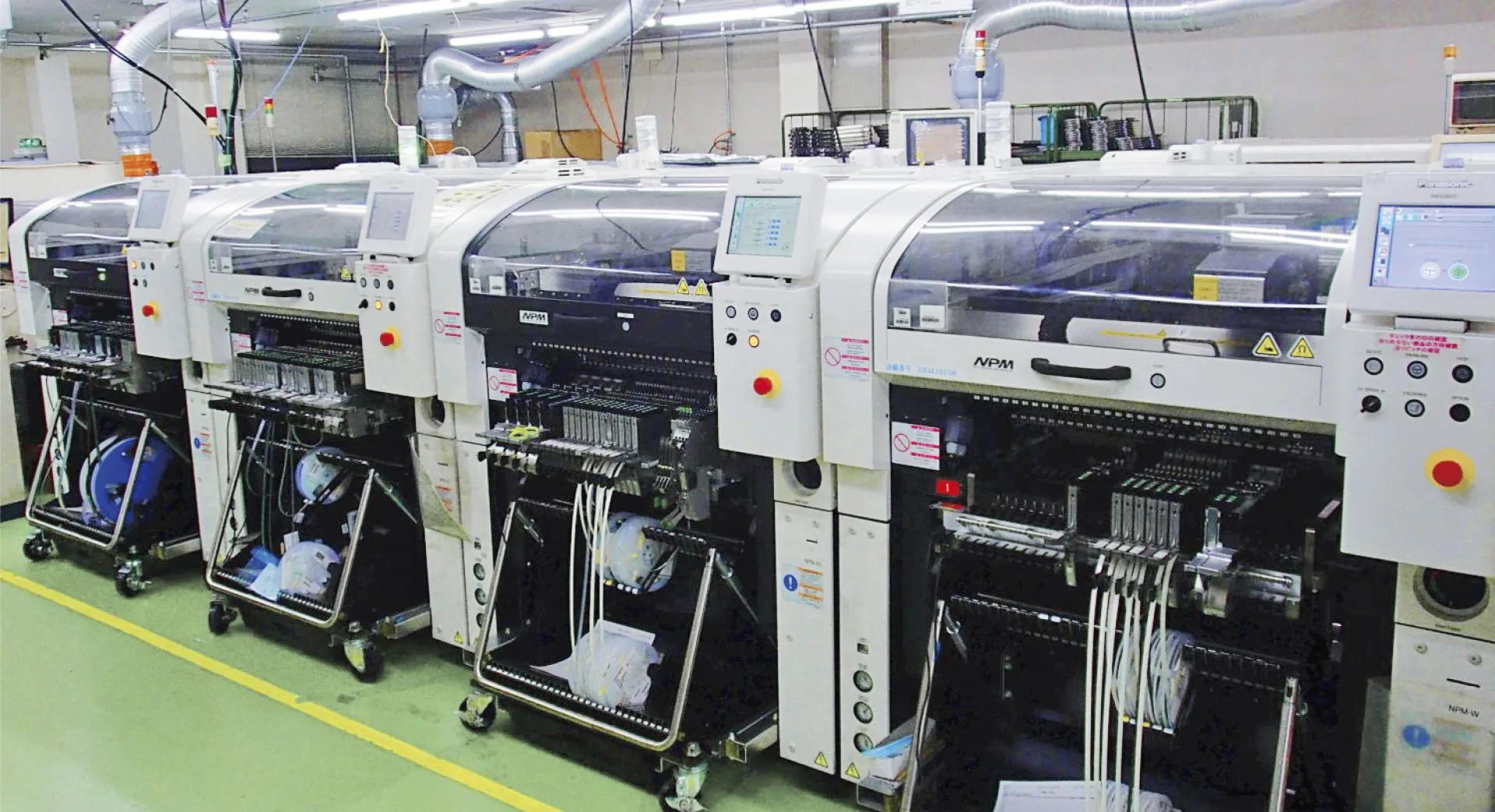
- Assembly: 0402 chips, 0.4 mm pitch CSP, BGA and LGA with X-ray inspection
Prototype PCB lead times
| Layers | Lead time | Data received by |
|---|---|---|
| 2 to 8 layers | 1.1 days | 20:00 |
| 10 to 14 layers | 1.1 days | 16:00 |
| 16 to 18 layers | 2.1 days | 16:00 |
| 20 to 24 layers | 3.1 days | 16:00 |
An express fee applies to short lead times.
Company
- Name
- 3B-OFFICE (株式会社サンビーオフィス)
- Address
- 4-34-1 Mataho-cho, Nishi-ku, Nagoya, Aichi 451-0014, Japan
- Representative
- President, 漆崎聖也
- Established
- January 23, 1987
- Certification
- ISO 9001, ISO 14001
- Contact
- TEL +81-52-522-0771 / FAX +81-52-522-0772